FPGA · 2026
TF Card Reader and VGA Display
An FPGA-based TF card reader on the DE1-SoC that parses FAT32 and displays images over VGA, with a custom breakout PCB and a layered UVM verification environment.
1.Overview
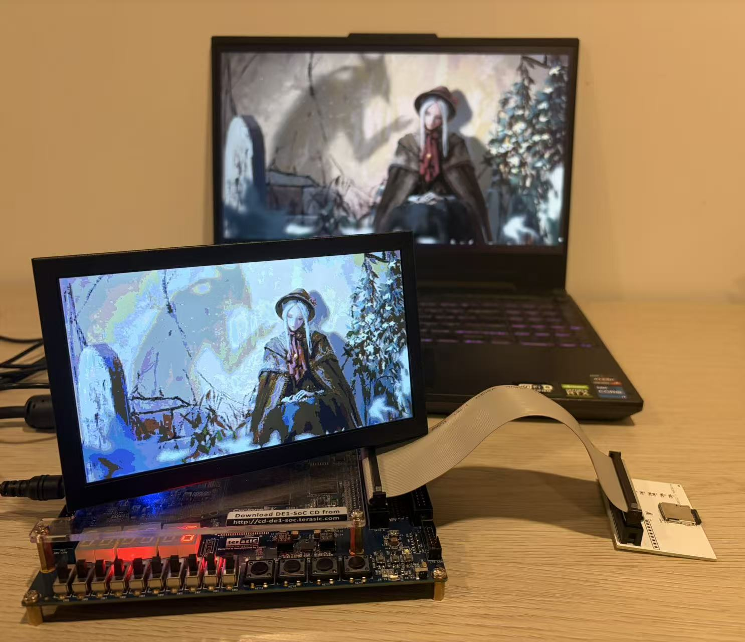
This project implements a TF card image reader and VGA display system on the DE1-SoC FPGA board using SystemVerilog. The design accesses a TF card in SD Native 1-bit mode, parses its FAT32 file system, and automatically locates IMAGE.BIN. A 320 × 240 image in RGB332 format is loaded into on-chip RAM and displayed at 640 × 480 resolution and 60 Hz using 2× pixel scaling.
The project combines synthesizable RTL, a custom TF card breakout PCB, a layered UVM verification environment, and Python image generation and preview utilities. Together, these components support development from test-image preparation and simulation through FPGA programming and hardware validation.
2.System Architecture
The system is organized as a sequence of modules that handle card communication, sector access, file-system parsing, image storage, and display timing. The main data path is TF Card → sdcmd_ctrl → sd_reader → sd_file_reader → img_ram → vga_ctrl → VGA. The top_sd_vga module integrates these blocks into the complete design.
The sdcmd_ctrl module sends SD commands and receives responses, while sd_reader manages card initialization and sector reads. The sd_file_reader module interprets FAT32 structures and locates the image file. Image bytes are written into img_ram, and vga_ctrl reads the buffered pixels to generate the VGA output. Buffering the image separates card access from the timing requirements of the display.
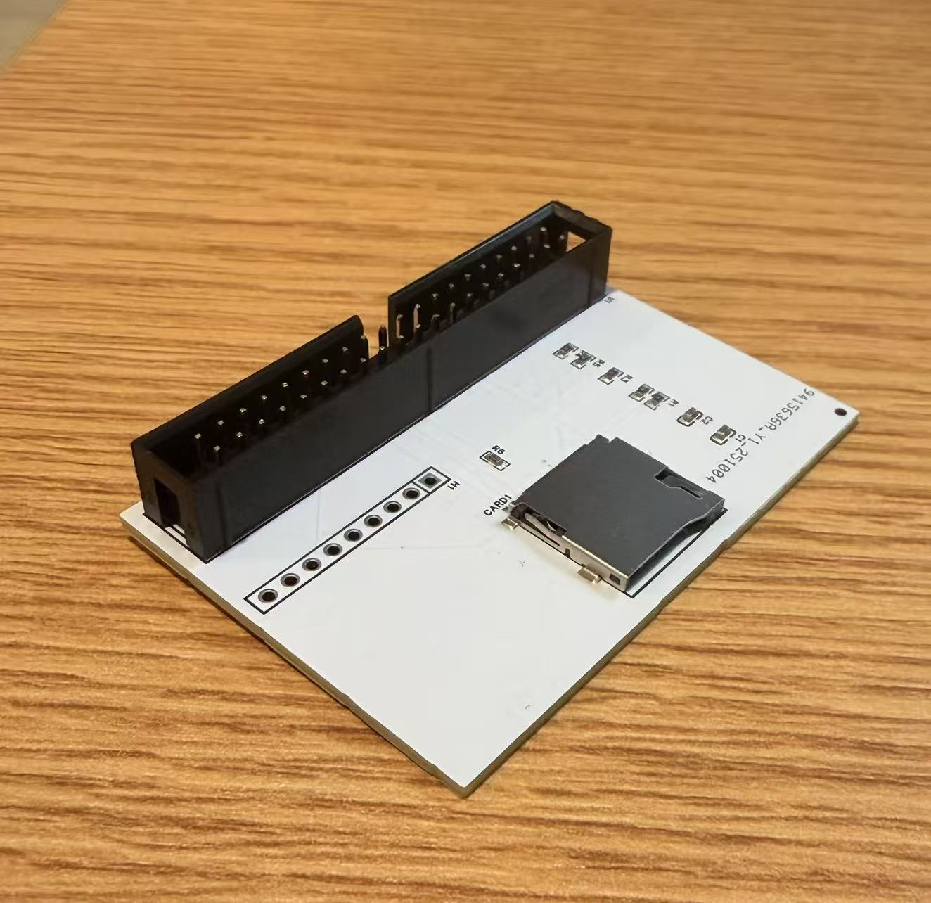
The DE1-SoC’s onboard TF card slot is connected directly to the Hard Processor System (HPS), so it is not available as a direct FPGA interface. A custom breakout PCB routes the card signals to the FPGA-accessible 40-pin GPIO header. The hardware deliverables include the schematic, bill of materials, and Gerber files for the adapter.
3.Detailed Design
SD Card Interface: The controller implements the native initialization sequence using CMD0, CMD8, CMD55, ACMD41, CMD2, CMD3, CMD7, and CMD16. After initialization, CMD17 performs single-block reads, with card data captured through DAT0 in 1-bit mode. Command handling and sector reading are separated into dedicated modules to make protocol behavior easier to develop and verify.
FAT32 File Reader: The file reader parses the master boot record, boot sector, root directory, and file data to locate IMAGE.BIN automatically. The expected file contains 320 × 240 pixels stored as RGB332, with one byte per pixel and a total size of 76,800 bytes. This gives the image reader and display controller a fixed data format.
Image Buffer and VGA Output: The image is stored in on-chip RAM before display. The VGA controller generates a 640 × 480 output at 60 Hz and scales the source image by repeating each pixel across two output columns and two output rows. RGB332 provides a compact representation with three bits for red, three for green, and two for blue.
Verification and Image Utilities: A layered UVM environment, organized from Layer1 to Layer3, accompanies the RTL for simulation in QuestaSim. Python utilities generate gradient, checkerboard, stripe, and ramp images in the required binary format. A separate preview utility allows the image data to be inspected before it is copied to the card.
4.Deployment
Prepare the Image: Use generate_image_bin.py to create IMAGE.BIN and inspect it with view_image_bin.py. Copy the 76,800-byte image file to a TF card formatted as FAT32, retaining the exact file name expected by the hardware reader.
Build and Program the FPGA: Create a project in Intel Quartus Prime Lite 18.1, add the source files from the RTL directory, and select top_sd_vga as the top-level entity. Apply the supplied pin assignment Tcl script, compile the design, and program the generated bitstream onto the DE1-SoC using USB-Blaster.
Connect and Run: Connect the breakout PCB to the DE1-SoC GPIO header using a 40-pin ribbon cable, attach a VGA monitor, and insert the prepared TF card. Press KEY0 to reset the design and begin initialization, file loading, and display. Correct TF card DAT pin mapping was essential to achieving a complete image on the hardware.
Check Hardware Status: HEX0 = 6 indicates that the file reader has reached DONE. LEDR0 indicates that IMAGE.BIN was found, and LEDR1 indicates that image reading has completed. LEDR6 is a latched historical timeout indicator, so it may remain illuminated even after the image has been displayed successfully.
5.Conclusion
The completed design demonstrates an FPGA-based path from removable storage to VGA output, combining SD Native communication, FAT32 parsing, on-chip image buffering, and display timing. Hardware testing confirmed that the full IMAGE.BIN image could be displayed after correcting the TF card DAT pin mapping, highlighting the importance of checking physical connections alongside RTL behavior.
The modular architecture, layered verification environment, and image preparation utilities provide a foundation for further development and debugging. The project’s architecture and data flow were inspired by FPGA-SDcard-Reader; the repository states that its RTL was independently implemented. The hardware demonstration uses Bloodborne fan art by wlop.