FPGA · 2025
Deep Neural Network Accelerator on FPGA
An FPGA acceleration platform for MNIST handwritten digit recognition, combining a Nios II processor, Q16.16 arithmetic, custom Avalon accelerators, and VGA output.
1.Overview
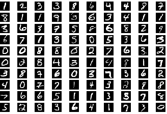
This project develops an FPGA-based acceleration platform for recognizing handwritten digits from the MNIST dataset. A Nios II embedded processor runs the control software, while custom SystemVerilog peripherals support memory transfers and fixed-point dot-product computation. The system targets the DE1-SoC board and combines processor software, external memory, and dedicated hardware within a single system-on-chip design.
The inference workload is a multilayer perceptron with 784 inputs, two hidden layers of 1,000 neurons each, and 10 outputs corresponding to digits 0–9. Each 28 × 28 grayscale image is flattened into an input vector, processed through weighted sums and biases, and classified by selecting the largest output. ReLU activation maps negative hidden-layer values to zero. Pretrained parameters and formatted test images provide the workload, allowing the project to focus on inference hardware and system integration.
2.System Architecture
The system is built in Platform Designer around a Nios II soft processor, 32 KB of on-chip program memory, an external SDRAM controller, and an Avalon memory-mapped interconnect. The processor executes the application from on-chip memory, while the 64 MB SDRAM holds network weights, biases, input images, and intermediate activations. JTAG supports program loading and debugging, and a JTAG UART provides a channel for diagnostic output.
The reference clocking design uses a PLL with a 50 MHz input and two 50 MHz outputs. One clocks the processor and peripheral logic; the other drives the external SDRAM with a −3 ns phase shift to account for board-level timing. The SDRAM clock uses zero phase shift in simulation. Keeping the PLL independent of the processor’s debug reset allows the clock source to remain active during program loading and debugging.
The custom accelerators expose CPU-facing configuration registers and memory-facing Avalon master interfaces. Software writes buffer addresses and operation lengths, starts an operation, and reads the completion or result register. A VGA peripheral provides grayscale image output, while a seven-segment display provides a simple interface for the recognized digit or test status.
3.Detailed Design
Q16.16 Arithmetic: Weights, biases, and activations use signed 32-bit Q16.16 fixed-point values, with a resolution of 1/65,536. Multiplication produces a 64-bit intermediate, which is shifted right by 16 bits to restore the original scale. The arithmetic uses truncation rather than rounding. Matching the software and hardware treatment of signed values and fractional bits is essential to obtaining consistent inference results.
Avalon Communication: The memory interface must distinguish between acceptance of a request and arrival of its data. The waitrequest signal indicates that a transaction must wait, while readdatavalid identifies a valid read response. SDRAM refresh and access latency can delay either stage. The accelerator control logic must therefore coordinate requests and responses instead of assuming that a memory read completes in one cycle.
Memory-Copy Accelerator: The word-copy peripheral moves blocks of aligned 32-bit words between memory locations. Software supplies a destination address, source address, and word count, then writes the start register. The hardware performs the read-and-write sequence, and a subsequent read of the completion register blocks until the transfer finishes. This provides a reusable hardware path for moving data without a processor-executed copy loop.
Dot-Product Accelerator: The dot-product peripheral receives the addresses of a weight vector and an activation vector, together with their length. It fetches the operands from memory and accumulates their fixed-point products. Software reads the result after completion, adds the neuron bias, and applies ReLU where required. Repeating this operation across the neurons implements the matrix-vector computation for a network layer.
VGA Visualization: A memory-mapped wrapper connects the processor to an eight-bit grayscale VGA core. Each pixel command packs its horizontal coordinate, vertical coordinate, and brightness into a single 32-bit write. A C plotting function provides the software interface, and a weighted neighborhood filter offers a way to transform a binary test image into shades of gray.
Data-Reuse Extension: The reference design proposes two on-chip SRAM banks for activation storage. Alternating the banks between layer inputs and outputs would allow activations to be reused across many neurons without repeatedly fetching them from SDRAM. A second accelerator master port could read activations from SRAM concurrently with weights from SDRAM. An optional further extension combines dot products, bias addition, ReLU, and result writeback in hardware. These are extension paths beyond the local repository’s implemented word-copy and basic dot-product modules.
4.Deployment
Build the Processor System: Configure the processor, program memory, PLL, SDRAM controller, and peripherals in Platform Designer. Assign their address ranges, connect clocks and resets, and export the board-facing SDRAM and VGA signals. Generate the system HDL, add the top-level design and timing constraints to Quartus, and compile the FPGA configuration.
Load the Application and Data: Use the Intel FPGA Monitor Program to program the board and load the Nios II application. Load nn.bin as binary data at SDRAM address 0x08000000 and a selected test image at 0x08800000. The application selects the software or accelerator path, processes the input, and uses the display peripherals for visual feedback.
Verify the Interfaces and Arithmetic: Test the VGA wrapper and accelerators individually before running the complete processor system. Memory-interface models can exercise delayed responses and stalled requests, while arithmetic tests compare fixed-point results against a software reference. System-level ModelSim simulation requires the generated processor modules, memory initialization files, and functional SDRAM model.
The checked-in application currently selects a memory-copy test, and its layer routine still calls the software dot-product implementation. Running fully accelerated inference therefore requires enabling and connecting the hardware path, then comparing its outputs with the reference model. Classification accuracy and acceleration should be reported only after those tests and timing measurements are completed.
5.Conclusion
This project connects neural network computation with practical FPGA system design. The main challenge extends beyond multiplication and accumulation to include memory latency, bus handshaking, fixed-point consistency, clock generation, and coordination between embedded software and custom peripherals.
The implemented memory-copy and dot-product modules provide the basis for progressively accelerating the inference workload. The next stage is complete inference validation and performance measurement, followed by exploring activation reuse in on-chip SRAM and integrating more of each layer’s computation into hardware.